
IGBT packages and solder paste layer voids - what's the connection?
2023-10-26
Stacking packaging technology is used in the IGBT to improve packaging density, as well as shorten the wire connections between chips, thereby improving the operating speed of the device by determining its safety. This structure has, however, seriously hampered the reliability of IGBT. What is the relationship between the IGBT package and the solder paste layer void? Read this article to find out.
What Is the Manufacturing Process of IGBT Module?
Here is a brief demonstration of the manufacturing process of the IGBT module.
Screen printing➔Automatic mouting/placement➔Vacuum reflow soldering➔Ultrasonic cleaning➔Defect detection (X-ray)➔Automatic wire bonding➔Laser marking➔Shell plastic sealing➔Housing potting and curing➔Terminal forming➔Functional testing
Screen printing➔Automatic mouting/placement➔Vacuum reflow soldering➔Ultrasonic cleaning➔Defect detection (X-ray)➔Automatic wire bonding➔Laser marking➔Shell plastic sealing➔Housing potting and curing➔Terminal forming➔Functional testing
IGBT Packaging Technology
As an important core device of power electronics, IGBT’s reliability is the most important factor in determining the safe operation of the entire device. Since the IGBT adopts stacked packaging technology, this technology not only improves the packaging density, but also shortens the interconnection length of the wires between chips, thereby improving the operating speed of the device.
But because of this structure, the reliability of IGBT has been seriously challenged. Since the IGBT is mainly used to switch the current, it will generate a large power loss, so heat dissipation is an important factor affecting its reliability.
But because of this structure, the reliability of IGBT has been seriously challenged. Since the IGBT is mainly used to switch the current, it will generate a large power loss, so heat dissipation is an important factor affecting its reliability.
What Is the Relationship Between the IGBT Package and Solder Paste Layer Void?
Solder layer voids are an important factor affecting the reliability of IGBTs
The primary failure points in IGBT module packaging are typically associated with the bonding wire connection, chip welding site, and substrate welding location. Among these, the two solder joints serve as the primary heat transfer pathways for IGBT, and the solder joint quality is the pivotal factor influencing its reliability.
Research has indicated that the presence of voids within the solder layer can disrupt the temperature cycling process and diminish the device's heat dissipation performance. This, in turn, leads to an escalation in taemperature and a disturbance in the working process's thermal cycle. Consequently, it results in localized overheating, expediting module damage.
According to a survey, for every 10°C increase in operating temperature, the failure rate due to temperature-related issues doubles. Furthermore, a hysteresis effect is observed in the relationship between stress and strain. During continuous temperature cycling, the material's shape undergoes real-time changes, amplifying the thermal fatigue experienced by the solder layer. Hence, in IGBT packaging, the critical focus should be on minimizing voids within the solder layer.
The reason why the IGBT soldering layer is prone to voids
IGBT chips are typically very large, measuring between 10mm and 20mm in length, and the size of the DBC is usually 20mm to 40mm. The generation of voids in the solder layer is mainly caused by volatiles in the solder material remaining in the solder layer. Due to the large welding area, volatiles in welding materials are very difficult to evaporate.
Therefore, the void in the IGBT solder layer has become a problem that engineers try to solve. For the high reliability requirements of IGBTs, the void rate must be an important control factor in the packaging process. A general IGBT for a small household appliance or general electrical device needs to have a void rate of 5%. For rail transit and aerospace, the requirements are even more stringent, and they must even fall below 0.1 percent.
1) Form of welding material
1. Solder tab: It is the most widely used solder in the field of IGBT.
1) Form of welding material
1. Solder tab: It is the most widely used solder in the field of IGBT.
Advantages: fewer organic components are used, and the void is low.
Disadvantages:
- Inconvenient to operate;
- Each product requires a specific size of solder tab.
2. Solder paste: It is a measure that has gradually emerged in the field of IGBT packaging in recent years.
Advantages: easy operation, low cost, suitable for welding of products of various specifications.
Advantages: easy operation, low cost, suitable for welding of products of various specifications.
Disadvantages:
- Volatilization of a large amount of organic components can easily cause voids;
- Residues must be cleaned.
To promote the volatilization of volatiles in solder paste, the solder paste is usually printed into several rectangular arrays, especially between the substrate and DBC, in order to use solder paste soldering. As a result of the channels between the solder paste, volatiles will be able to evaporate. The solder paste's volatility and wettability should be well matched with the process in order to avoid voids in the trench.
2) Welding process
1. One-time packaging: DBC/substrate and DBC/chip are placed with solder at the same time, and the soldering is realized at the same time through one furnace.
Advantages: high efficiency;
1. One-time packaging: DBC/substrate and DBC/chip are placed with solder at the same time, and the soldering is realized at the same time through one furnace.
Advantages: high efficiency;
Disadvantage: The two layers of solder melt at the same time, and the ceramic chip floats between the upper and lower layers of molten solder, which increases the difficulty of void discharge.
2.Ladder packaging: first solder the DBC/substrate with high-melting-point solder, and then use low-melting-point solder for secondary soldering between the DBC/chip (during the secondary soldering, the solder in the first soldering does not melt).
Advantages: Avoid DBC floating between molten solder, low void rate;
Disadvantages: low production efficiency.
3) Selection of welding furnace
IGBT products with high requirements need to be welded in a vacuum furnace. The vacuum negative pressure is also conducive to the release of volatiles in solder paste. It is, however, important to match the vacuum degree and vacuum timing with the solder paste, otherwise it is difficult to achieve the desired result.
There is also the option of curing a low viscosity, high transparency silicone gel at room temperature, which is moisture-resistant, shock-resistant, temperature-resistant, and self-healing. IGBT modules and other precision electronic components are mainly sealed and potting with this material.
- Soft and elastic colloid after curing, jelly-like gel, good adhesion and sealing performance to many substrates;
- High and low temperature resistance (-60°C-240°C), and has excellent electrical insulation properties;
- Highly transparent, easy to repair, and can heal automatically after the colloid is broken.
Conclusion
IGBT packaging and solder paste layer voids have been explained in the above illustration. As you can see, voids of solder paste are essential for IGBT packaging. If we cannot handle the void issue better, it may have a significant impact on IGBT packaging. Chengliankaida Technology.co., LTD. was founded in 2007 and has amassed over 16 years of experience in PCB and PCB assembly. We specialize in the research and development of a series of vacuum welding machines and production lines for semiconductor device packaging. Our comprehensive one-stop services, encompassing design, manufacturing, assembly, testing, and delivery, are committed to providing you with a highly satisfactory service.

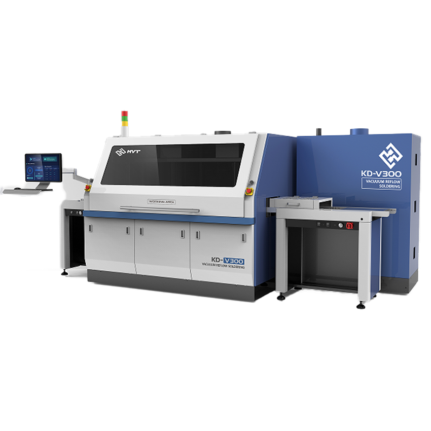

Reflow Ovens for Solder Paste and Pcb Assembly
Research Report on Advantages of Chinese Vacuum Reflow Soldering Equipment in Germany
Related Article

Explore laser packaging process routes for LiDAR and optoelectronics. Discover how vacuum eutectic soldering secures sub-micron alignment stability.
Laser Diode Packaging Technologies: From TO-Can to Silicon Photonics

Compare inline vs. batch vacuum soldering systems. Learn how vacuum reflow ovens optimize void-free welding for high-power semiconductor packaging.
Vacuum Soldering Process & Equipment Comparison: How to Achieve Automotive-Grade Low-Void Manufacturing

