
What Are the Defects of Soldering?
2024-01-15
Wave soldering represents a large-scale soldering technique employed in the assembly of electronic components onto a printed circuit board (PCB) to form a cohesive electronic assembly. This method derives its name from the utilization of waves of molten solder to affix metal components to the PCB. The process involves a tank containing molten solder, into which the components are inserted onto the PCB. Subsequently, the loaded PCB traverses a pumped wave or cascade of solder. The molten solder adheres to the exposed metallic areas of the board, excluding those protected by solder mask—a shielding coating that prevents solder from connecting between connections. This results in a reliable mechanical and electrical connection. Compared to manual soldering, wave soldering is a considerably faster process and can yield a higher quality product.
Wave soldering finds application in both through-hole printed circuit assemblies and surface mount assemblies. In the latter scenario, components are affixed to the printed circuit board surface using adhesive placement equipment before undergoing the passage through the molten solder wave.
In this blog post, we will discuss the most common PCB soldering defects and their causes, as well as how these defects affect the assembly process and technologies for reducing or eliminating them.
Wave soldering finds application in both through-hole printed circuit assemblies and surface mount assemblies. In the latter scenario, components are affixed to the printed circuit board surface using adhesive placement equipment before undergoing the passage through the molten solder wave.
In this blog post, we will discuss the most common PCB soldering defects and their causes, as well as how these defects affect the assembly process and technologies for reducing or eliminating them.
Common Types of PCB Soldering Defects
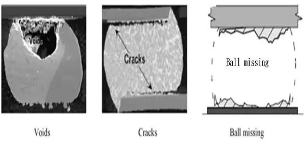
PCB (Printed Circuit Board) soldering defects can arise during the assembly process, impacting the functionality and reliability of electronic devices. Identifying and understanding these defects is crucial for maintaining the quality of electronic assemblies. Here are some common types of PCB soldering defects:
1.Solder Bridging
- Description: Unintended connections or bridges of solder between adjacent solder joints.
- Cause: Excessive solder applied, incorrect spacing of components, or improper solder mask application.
- Effect: Short circuits, affecting the functionality of the circuit.
2.Solder Balling
- Description: Formation of small solder balls on the PCB surface or between components.
- Cause: Excess solder paste, incorrect reflow temperature, or inadequate cleaning.
- Effect: Risk of short circuits, especially in fine-pitch components.
3.Tombstoning
- Description: One end of a surface mount component lifts, resembling a tombstone.
- Cause: Imbalance in solder paste volume, uneven heating during reflow, or component misalignment.
- Effect: Misalignment can lead to poor electrical connections or open circuits.
4.Insufficient Solder
- Description: Incomplete or insufficient solder coverage on the joint.
- Cause: Insufficient solder paste, inadequate heating during reflow, or poor solderability of components.
- Effect: Weak or unreliable connections, leading to electrical failure.
5.Cold Solder Joint
- Description: Solder does not fully wet the surfaces, resulting in a dull, grainy appearance.
- Cause: Insufficient heating during soldering, inadequate flux, or contamination.
- Effect: Reduced mechanical strength and poor electrical conductivity.
6.Lifted Pads or Traces
- Description: Pads or traces detach from the PCB surface.
- Cause: Excessive heat, poor adhesion, or incorrect material selection.
- Effect: Loss of connectivity and functionality.
7.Component Misalignment
- Description: Components are not correctly placed on the PCB.
- Cause: Issues with pick-and-place machines, inaccurate placement, or inadequate inspection.
- Effect: Incorrect functionality, potential short circuits, or open connections.
8.Overheating
- Description: Excessive heat during soldering damages components or the PCB.
- Cause: Prolonged exposure to high temperatures, incorrect soldering profiles, or inadequate cooling.
- Effect: Component failure, reduced lifespan, or degraded performance.
9.Voiding
- Description: Formation of voids or air pockets within the solder joint.
- Cause: Trapped gases during solder reflow, inadequate flux, or incorrect solder paste composition.
- Effect: Reduced mechanical strength and compromised electrical conductivity.
10.Flux Residue
- Description: Residual flux material left on the PCB after soldering.
- Cause: Inadequate cleaning, improper flux selection, or excessive flux application.
- Effect: Potential corrosion, electrical leakage, or reduced reliability.
Step by Step Solutions of PCB Soldering Defects
Addressing and resolving PCB soldering defects requires a systematic approach to ensure the quality and reliability of electronic assemblies. Here are step-by-step solutions for common PCB soldering defects:
1. Solder Bridging

Reduce Solder Volume: Adjust the solder volume to prevent excess solder.
Optimize Spacing: Ensure proper component spacing to minimize the risk of bridging.
Refine Solder Mask Application: Improve solder mask application to protect against unintended bridges.
Optimize Spacing: Ensure proper component spacing to minimize the risk of bridging.
Refine Solder Mask Application: Improve solder mask application to protect against unintended bridges.
2. Excess of Solder
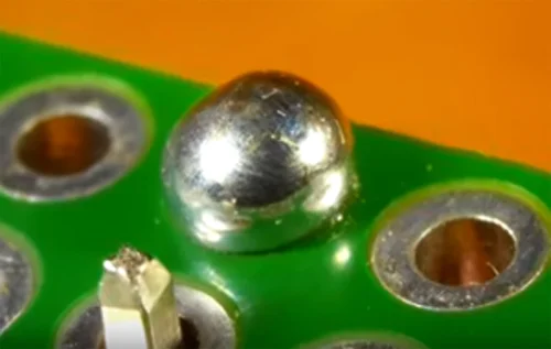
Optimize Solder Paste Application: Apply an appropriate amount of solder paste during the stencil printing process.
Monitor Reflow Temperature: Ensure the correct reflow temperature to prevent excess solder.
Monitor Reflow Temperature: Ensure the correct reflow temperature to prevent excess solder.
3. Balling of Solder

Control Solder Paste Quantity: Apply an optimal amount of solder paste to prevent balling.
Adjust Reflow Conditions: Optimize reflow conditions, including temperature and duration.
Adjust Reflow Conditions: Optimize reflow conditions, including temperature and duration.
4. Heat Loss Analysis
Enhance Heating Processes: Ensure proper heating during soldering to minimize heat loss.
Optimize Thermal Profiling: Fine-tune thermal profiles for consistent and adequate heating.
Optimize Thermal Profiling: Fine-tune thermal profiles for consistent and adequate heating.
5. Tombstoning

Balance Solder Paste Volume: Adjust solder paste volume to prevent imbalances.
Ensure Even Heating: Optimize reflow conditions to promote even heating.
Ensure Even Heating: Optimize reflow conditions to promote even heating.
6. Pins and Connector Connections
Ensure Proper Alignment: Implement precise alignment during component placement.
Improve Soldering Quality: Enhance soldering processes to ensure robust pin and connector connections.
Improve Soldering Quality: Enhance soldering processes to ensure robust pin and connector connections.
7. Surface Mount Issues
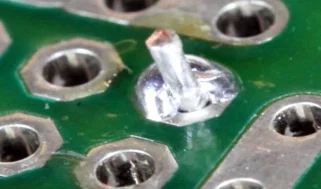
Enhance Adhesion Processes: Improve the adhesion of surface mount components.
Verify Placement Accuracy: Ensure accurate placement of surface mount components.
Verify Placement Accuracy: Ensure accurate placement of surface mount components.
8. Skips Solder
Optimize Solder Paste Application: Apply sufficient solder paste for complete coverage.
Monitor Heating Conditions: Ensure proper heating during the reflow process.
Monitor Heating Conditions: Ensure proper heating during the reflow process.
9. Lift Pads

Control Heating Parameters: Avoid excessive heat during soldering.
Enhance Adhesion: Improve pad adhesion to prevent detachment.
Enhance Adhesion: Improve pad adhesion to prevent detachment.
What Are the Effects of These Defects on the Assembly Process?
These imperfections can lead to various issues throughout the assembly process, ranging from aesthetic concerns to functional failures. While some issues can be addressed through straightforward rework, others may necessitate discarding the entire board. This not only introduces delays in the assembly process but also results in elevated costs.
Methods and Technologies That Help Catch Assembly Errors
Various inspection and testing methods are employed to detect soldering defects, including the following:
1.Electrical Part Verification
Automated optical inspection systems are used to scrutinize soldering defects.
2.X-Ray Inspection
Utilizes X-rays to examine PCBs for soldering defects, especially beneficial for detecting smaller defects in solder joints. This method is particularly valuable for ensuring uniform quality across multiple board builds.
3.Flying Probe Test (FPT)
Employs probes to test PCBs for electrical continuity and shorts. Spring-loaded probes move along the pads and traces, applying pressure to assess integrity.
4.In-Circuit Test (ICT)
Utilizes a bed of nails fixture to examine continuity, signal strength, voltage levels, resistance, and more. Ensures error-free assembly during the soldering process.
5.3D Optical Inspection
Utilizes lasers to scan the PCB, creating a three-dimensional image for detecting small defects.
6.Automated Optical Inspection (AOI)
Uses automated optical inspection systems to identify soldering defects.
7.Paste Inspection
An effective method for inspecting solder paste application process, ensuring the absence of defects.
8.Design Review
After the design process, a comprehensive design review is conducted to identify potential issues leading to soldering defects. This includes:
1.Electrical Part Verification
Automated optical inspection systems are used to scrutinize soldering defects.
2.X-Ray Inspection
Utilizes X-rays to examine PCBs for soldering defects, especially beneficial for detecting smaller defects in solder joints. This method is particularly valuable for ensuring uniform quality across multiple board builds.
3.Flying Probe Test (FPT)
Employs probes to test PCBs for electrical continuity and shorts. Spring-loaded probes move along the pads and traces, applying pressure to assess integrity.
4.In-Circuit Test (ICT)
Utilizes a bed of nails fixture to examine continuity, signal strength, voltage levels, resistance, and more. Ensures error-free assembly during the soldering process.
5.3D Optical Inspection
Utilizes lasers to scan the PCB, creating a three-dimensional image for detecting small defects.
6.Automated Optical Inspection (AOI)
Uses automated optical inspection systems to identify soldering defects.
7.Paste Inspection
An effective method for inspecting solder paste application process, ensuring the absence of defects.
8.Design Review
After the design process, a comprehensive design review is conducted to identify potential issues leading to soldering defects. This includes:
- Design for Manufacturability (DFM) Analysis: Identifies areas for improvement in the design to prevent soldering defects.
- DFX (Design for Excellence) Analysis: Identifies design aspects that can be enhanced to prevent soldering defects.
The implementation of these inspection and testing methods contributes to the enhancement of PCB quality and the prevention of soldering defects. PCB manufacturers can leverage these techniques to refine their manufacturing processes and deliver high-quality products.
Conclusions
For PCB soldering defects, proactive prevention proves to be the most effective remedy. Employing various technologies and methods allows the identification of potential defects before they manifest into issues, ultimately saving both time and money in the long term. Rather than waiting for problems to arise, adopting a proactive approach to prevent soldering defects is paramount.
A Guide to Online Vacuum Reflow Soldering Furnace
Best Vaccum Reflow Oven KD-V43 for Sale
Related Article

Explore laser packaging process routes for LiDAR and optoelectronics. Discover how vacuum eutectic soldering secures sub-micron alignment stability.
Laser Diode Packaging Technologies: From TO-Can to Silicon Photonics

Compare inline vs. batch vacuum soldering systems. Learn how vacuum reflow ovens optimize void-free welding for high-power semiconductor packaging.
Vacuum Soldering Process & Equipment Comparison: How to Achieve Automotive-Grade Low-Void Manufacturing

