
What's the Difference Between Reflow and Wave Soldering?
2024-03-19
As a component of PCBA manufacture, soldering is essential since it joins the components to the board. However, the soldering process may vary as there are several soldering processes.
In the industry, wave soldering and reflow soldering are the most commonly used soldering methods. It is important to understand the differences between these soldering processes in order to determine which one is appropriate for your PCBA. Most of the time, beginners and new buyers get confused about them.
Here's a closer look at the differences between reflow soldering and wave soldering. But first, let's take a look at how these processes work.
Here's a closer look at the differences between reflow soldering and wave soldering. But first, let's take a look at how these processes work.
What Is Reflow Soldering?

Reflow soldering is a commonly used process in electronics manufacturing for soldering surface-mount components onto printed circuit boards (PCBs). It involves melting solder paste, a mixture of tiny solder particles and flux, to create electrical connections between the components and the PCB pads.
Here's how the reflow soldering process typically works:
1.Application of solder paste: A stencil is used to apply solder paste onto the PCB, depositing it onto the pads where the surface-mount components will be placed. The solder paste is a mixture of tiny solder particles and flux, which helps remove oxides and promotes solder wetting.
2.Component placement: Surface-mount components, such as resistors, capacitors, integrated circuits, and other electronic parts, are placed onto the solder paste on the PCB according to the design specifications.
3.Heating in a reflow oven: The PCB with the components and solder paste is then transferred to a reflow oven. The oven has precise temperature control zones to gradually heat the assembly through a series of stages:
a. Preheating: The PCB is gradually heated to a temperature below the melting point of the solder paste, allowing the flux to activate and remove any moisture and contaminants.
b. Reflow: Once the PCB reaches a specific temperature, typically above the melting point of the solder paste, the solder particles liquefy, forming metallurgical bonds between the component leads and the PCB pads.
c. Cooling: After the solder has reflowed and solidified, the PCB is cooled gradually to prevent thermal shock and ensure the integrity of the solder joints.
a. Preheating: The PCB is gradually heated to a temperature below the melting point of the solder paste, allowing the flux to activate and remove any moisture and contaminants.
b. Reflow: Once the PCB reaches a specific temperature, typically above the melting point of the solder paste, the solder particles liquefy, forming metallurgical bonds between the component leads and the PCB pads.
c. Cooling: After the solder has reflowed and solidified, the PCB is cooled gradually to prevent thermal shock and ensure the integrity of the solder joints.
4.Inspection: After cooling, the PCB is inspected to ensure that all components are properly soldered and aligned. Any defects or soldering issues may be identified and rectified at this stage.
Reflow soldering offers several advantages over traditional soldering methods, such as wave soldering:
- It is well-suited for small and complex surface-mount components.
- It enables precise control over soldering temperature profiles, reducing the risk of thermal damage to sensitive components.
- It produces cleaner and more consistent solder joints with minimal flux residue.
- It allows for high-throughput production with automated equipment, improving efficiency and scalability.
What is Wave Soldering?
Wave soldering is a common method used in electronics manufacturing for soldering through-hole components onto printed circuit boards (PCBs). Unlike reflow soldering, which is primarily used for surface-mount components, wave soldering is well-suited for through-hole components such as connectors, switches, and larger integrated circuits.
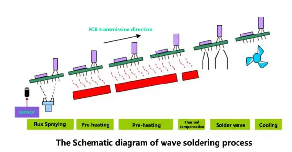
Here's how the wave soldering process typically works:
1.Flux application: Before soldering, a flux is applied to the PCB to remove oxides from the metal surfaces and promote solder wetting. Flux helps ensure a reliable solder joint by improving the flow of solder and preventing oxidation during the soldering process.
2.Component placement: Through-hole components are inserted into pre-drilled holes on the PCB. The components are positioned on one side of the PCB, with their leads protruding through the opposite side.
3.Solder wave preparation: A pool of molten solder is prepared in a solder pot or wave soldering machine. The solder is typically a mixture of tin and lead (though lead-free solder is also used for environmental and safety reasons), melted at temperatures above its melting point.
4.Solder wave formation: Once the solder reaches the desired temperature, a pump or conveyor system creates a continuous wave of molten solder. The wave is precisely controlled to maintain the correct height and temperature, ensuring proper solder flow and coverage.
5.Soldering process: As the PCB moves over the solder wave, the exposed metal leads of the through-hole components come into contact with the molten solder. The solder adheres to the exposed metal surfaces through capillary action, forming solid solder joints between the component leads and the PCB pads.
6.Cooling: After passing through the solder wave, the PCB is cooled to solidify the solder joints and prevent thermal damage to the components. Cooling may be achieved through various methods, such as air or water cooling.
7.Cleaning: Once the solder joints have solidified, the PCB may undergo a cleaning process to remove any flux residues or contaminants left behind from the soldering process. This ensures the reliability and integrity of the solder joints over the long term.
Wave soldering offers several advantages for soldering through-hole components:
- It is a high-speed and cost-effective method for soldering large volumes of PCBs with through-hole components.
- It provides consistent and reliable solder joints with good mechanical strength.
- It is suitable for a wide range of through-hole components and PCB sizes.
- It can be easily automated, allowing for efficient mass production.
Reflow Soldering vs Wave Soldering
Complexity
Wave soldering is renowned for its complexity. The process involves carefully placing the PCB onto a conveyor belt, which then passes over a solder wave. Achieving and adjusting the solder wave conditions require expertise and precision. Even a slight mishandling can compromise the quality of solder joints, making it imperative for the handler to be highly skilled.
Reflow soldering, in contrast, is comparatively simpler. The process involves applying solder paste onto the PCB using a stencil, followed by placing it into a reflow oven. The simplicity of reflow soldering makes it more accessible and less demanding in terms of expertise.
Environmental Conditions
Maintaining precise environmental conditions is critical in both reflow and wave soldering processes. In wave soldering, fluctuations in temperature or other environmental factors can directly impact the quality of solder joints formed by the molten solder wave. Similarly, in reflow soldering, stable environmental conditions are necessary to ensure consistent soldering results. Preheating the board and melting the solder paste require careful control of temperature to prevent defects and imperfections.
Constraints
Reflow soldering and wave soldering each present unique constraints. In reflow soldering, controlling the duration of the board under the solder wave is crucial. Exceeding or falling short of the specified time limits can result in soldering defects, such as excess solder or incomplete joints. Additionally, factors like pad shape, size, and orientation play significant roles in wave soldering.
Reflow soldering requires precision timing as well, but the constraints are generally less stringent compared to wave soldering.
Speed
Wave soldering is known for its speed, making it the preferred choice for large-volume PCB productions. The automated process involves spraying flux onto the PCBs, which then pass swiftly over the solder wave. In contrast, reflow soldering is relatively slower, as the PCBs spend time inside the reflow oven after solder paste application.
Cost
Wave soldering offers a cost-effective solution for large-volume orders due to its simplicity and efficiency. The equipment required for wave soldering is generally less expensive compared to reflow soldering. Reflow soldering, on the other hand, involves higher initial costs due to specialized stencil production and the expense of reflow ovens.
Usage
Wave soldering is ideal for through-hole components, where the solder wave can reliably form solder joints on component leads. Reflow soldering, on the other hand, is well-suited for surface-mount devices (SMDs), thanks to its precise control over solder paste application and reflow temperature.
Wave soldering is renowned for its complexity. The process involves carefully placing the PCB onto a conveyor belt, which then passes over a solder wave. Achieving and adjusting the solder wave conditions require expertise and precision. Even a slight mishandling can compromise the quality of solder joints, making it imperative for the handler to be highly skilled.
Reflow soldering, in contrast, is comparatively simpler. The process involves applying solder paste onto the PCB using a stencil, followed by placing it into a reflow oven. The simplicity of reflow soldering makes it more accessible and less demanding in terms of expertise.
Environmental Conditions
Maintaining precise environmental conditions is critical in both reflow and wave soldering processes. In wave soldering, fluctuations in temperature or other environmental factors can directly impact the quality of solder joints formed by the molten solder wave. Similarly, in reflow soldering, stable environmental conditions are necessary to ensure consistent soldering results. Preheating the board and melting the solder paste require careful control of temperature to prevent defects and imperfections.
Constraints
Reflow soldering and wave soldering each present unique constraints. In reflow soldering, controlling the duration of the board under the solder wave is crucial. Exceeding or falling short of the specified time limits can result in soldering defects, such as excess solder or incomplete joints. Additionally, factors like pad shape, size, and orientation play significant roles in wave soldering.
Reflow soldering requires precision timing as well, but the constraints are generally less stringent compared to wave soldering.
Speed
Wave soldering is known for its speed, making it the preferred choice for large-volume PCB productions. The automated process involves spraying flux onto the PCBs, which then pass swiftly over the solder wave. In contrast, reflow soldering is relatively slower, as the PCBs spend time inside the reflow oven after solder paste application.
Cost
Wave soldering offers a cost-effective solution for large-volume orders due to its simplicity and efficiency. The equipment required for wave soldering is generally less expensive compared to reflow soldering. Reflow soldering, on the other hand, involves higher initial costs due to specialized stencil production and the expense of reflow ovens.
Usage
Wave soldering is ideal for through-hole components, where the solder wave can reliably form solder joints on component leads. Reflow soldering, on the other hand, is well-suited for surface-mount devices (SMDs), thanks to its precise control over solder paste application and reflow temperature.
How Do I Decide Which Soldering Method to Use?
The choice of soldering method required is contingent upon several factors, including the components' type, size, and volume. Typically, boards encompass a combination of through-hole and surface-mount technology (SMT) components, necessitating the utilization of both soldering techniques. Consequently, multiple stages may be employed to accommodate the requirements of both methods.
Determining the appropriate soldering method is best achieved through consultation with your PCB manufacturer. Given the various considerations involved, it is advisable to seek guidance from experts who specialize in PCBA manufacturing. Attempting to make this decision independently may overlook crucial details. PCB manufacturers possess comprehensive expertise, gained through daily practice, enabling them to offer tailored recommendations suited to your specific needs.
Determining the appropriate soldering method is best achieved through consultation with your PCB manufacturer. Given the various considerations involved, it is advisable to seek guidance from experts who specialize in PCBA manufacturing. Attempting to make this decision independently may overlook crucial details. PCB manufacturers possess comprehensive expertise, gained through daily practice, enabling them to offer tailored recommendations suited to your specific needs.
What Is the Ideal Number of Zones for a Reflow Oven
What Is Solder Paste Inspection
Related Article

Explore laser packaging process routes for LiDAR and optoelectronics. Discover how vacuum eutectic soldering secures sub-micron alignment stability.
Laser Diode Packaging Technologies: From TO-Can to Silicon Photonics

Compare inline vs. batch vacuum soldering systems. Learn how vacuum reflow ovens optimize void-free welding for high-power semiconductor packaging.
Vacuum Soldering Process & Equipment Comparison: How to Achieve Automotive-Grade Low-Void Manufacturing

