
How to Avoid Five Types of Soldering Defects in PCB Assemblies
2023-12-25
Soldering defects in PCB assemblies can lead to performance issues and compromised functionality. In this comprehensive guide, we'll delve into the essential techniques and strategies to help you avoid five common soldering defects, ensuring the integrity and reliability of your printed circuit board (PCB) assemblies.
Five Types of Soldering Defects to be Aware Of
Solder defects can happen for a variety of reasons when manufacturing a printed circuit board. Here are five such reasons for PCB designers to be aware of:
1.Sunken joints
During wave soldering, molten solder will wick up into the holes of through-hole parts to solder the lead to the holes, however there is a danger that the solder will sink down through the holes, leaving behind a gap in the solder joint and the part is easily broken if it sinks down past the hole.
2.Solder shorts
It is becoming increasingly difficult for solders to short across some of these leads as lead pitches become smaller and smaller. It was not a problem when the lead pitches were 0.100” or 0.100” in size. Now that lead pitches have decreased from 0.050” to 0.025”, there is a greater chance that the solder will bridge between the leads.
It is becoming increasingly difficult for solders to short across some of these leads as lead pitches become smaller and smaller. It was not a problem when the lead pitches were 0.100” or 0.100” in size. Now that lead pitches have decreased from 0.050” to 0.025”, there is a greater chance that the solder will bridge between the leads.
3.Shadowing
During wave soldering, when a large component precedes a smaller part into the wave, the larger component will likely shadow the smaller component. This can result in an undesirable condition where the parts that are shadowed do not receive enough amount of solder due to the shadowing of the smaller component.
4.Tombstoning
When discrete components are being soldered through reflow, they can sometimes stand up on their end instead of being soldered to their respective pads on both ends. There is a thermal imbalance between the two pads that causes the solder paste on one pad to reflow more rapidly than the solder paste on the other, which pulls the part along with it as a result.
5.Incomplete joints
The airflow can be inhibited in the solder reflow oven if it is not allowed to flow properly, which can lead to certain parts not getting heated enough to form a good solder joint. In a similar way to what happens when parts shadow each other during wave soldering, this can also be caused by larger parts blocking smaller components.
Fortunately, there are steps that you can take while designing the circuit board that will prevent these problems from occurring.
Design Recommendations to Avoid Soldering Defects
Here are some design recommendations to make your PCB design have the best chance of forming good solder joints, and to help you improve the solderability of your PCB design:
It is important to use the recommended pad size for the drill hole that will be used when developing PCB component footprints for thru-hole parts. When the hole is too small for the thru-hole leads, it can lead to problems when inserting the part, while a hole that is too big can have the molten solder fall back down the hole before forming a successful solder joint.
When creating thru-hole pads for high-density parts such as connectors with fine-pitched leads, use an alternatively shaped pad to help with the soldering process. It has been shown that pad lengths that are increased on the side of the pad that will leave the wave will help control the tendency for solder bridging to occur.
If you work with your PCB contract manufacturer before you design your board, you will be able to determine which way the board will enter the wave. This will allow you to locate your surface mount components so that there is a reduced risk that larger components will shadow smaller ones when the board enters the wave.
Surface mount passives, particularly small surface mount passives, need to have appropriate thermal reliefs when they are connected to large metal planes. This is because a large metal plane that completely engulfs an SMT pad will act as a heat sink, which can cause a thermal imbalance that can cause tombstoning.
You should also be careful about placing tall components such as heat sinks and tantalum capacitors in the reflow oven so that they do not obstruct airflow to smaller parts, just as you would with wave soldering. It is in this manner that you can be sure that all parts will be evenly heated in the reflow oven so that good solder joints can be formed.
There are a number of different design methodologies that can be used to help improve the soldering process, and your PCB contract manufacturer will be able to assist you with determining which methodology will work best for your design.
Vacuum Reflow Oven for PCB Assembly
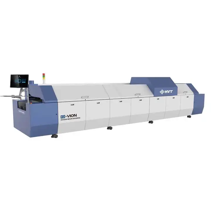
The KD-V8N Vacuum Reflow Soldering Oven stands as a cutting-edge solution for precise and efficient soldering processes in electronic manufacturing. With its advanced features and robust construction, this vacuum reflow oven is designed to meet the demands of modern PCB assembly, ensuring optimal soldering results and reliability.
Key Features:
1.Max Welding Size: The KD-V8N accommodates a broad range of PCB sizes, with a minimum of 150150mm and a maximum of 410470mm, providing flexibility for various electronic applications.
2.Preheating and Heating Zones: Equipped with 8 preheating zones both on the upper and lower sides, along with a lengthy 3800mm heating zone, this oven ensures uniform temperature distribution throughout the soldering process.
3.Cooling System: The KD-V8N features an efficient cooling system with 2 cooling zones on both the upper and lower sides, contributing to the stabilization of soldered components and preventing overheating.
4.Vacuum Technology: The inclusion of a vacuum zone with adjustable parameters such as minimum vacuum (10-100pa) and vacuum speed (40m³/h) allows for precise control over the soldering environment, ensuring high-quality results.
5.Flux Recovery System: This system reduces the frequency of equipment maintenance, leading to an extended service life for critical components. It enhances operational efficiency and minimizes downtime.
6.Control System: The KD-V8N boasts an intuitive control system featuring an industrial touch screen paired with Siemens PLC. Users can easily set and monitor various parameters, ensuring accurate and customizable soldering processes.
7.Conveyor System: With a conveyor net width of 450mm and an adjustable transmit track ranging from 50-400mm, the oven supports diverse PCB layouts. The chain transmit system, operating at speeds from 300-2000mm/min, ensures smooth and reliable transportation.
8.Temperature Control: The computer closed-loop temperature control, driven by SSR, offers precise control within a temperature range from room temperature to 350℃. The system maintains a temperature control accuracy of ±1℃, ensuring consistent and reliable soldering results.
9.Cooling Mechanism: The cooling mechanism employs a water cooling system, efficiently dissipating heat and contributing to the overall stability of the soldered components.
10.Alarm and Indication: The KD-V8N comes equipped with an alarm system that promptly notifies users of temperature anomalies. The 3-color light indication (Yellow for Heating, Green for Constant Temperature, Red for Temperature Anomaly) provides a quick visual status check.
11.External Systems: The oven integrates seamlessly with external systems, featuring air exhaust requirements of 10 cubic/min with 2 tubes of φ180mm, a nitrogen protector, and an external water-cooling system for enhanced performance.
Technical Specifications:
Key Features:
1.Max Welding Size: The KD-V8N accommodates a broad range of PCB sizes, with a minimum of 150150mm and a maximum of 410470mm, providing flexibility for various electronic applications.
2.Preheating and Heating Zones: Equipped with 8 preheating zones both on the upper and lower sides, along with a lengthy 3800mm heating zone, this oven ensures uniform temperature distribution throughout the soldering process.
3.Cooling System: The KD-V8N features an efficient cooling system with 2 cooling zones on both the upper and lower sides, contributing to the stabilization of soldered components and preventing overheating.
4.Vacuum Technology: The inclusion of a vacuum zone with adjustable parameters such as minimum vacuum (10-100pa) and vacuum speed (40m³/h) allows for precise control over the soldering environment, ensuring high-quality results.
5.Flux Recovery System: This system reduces the frequency of equipment maintenance, leading to an extended service life for critical components. It enhances operational efficiency and minimizes downtime.
6.Control System: The KD-V8N boasts an intuitive control system featuring an industrial touch screen paired with Siemens PLC. Users can easily set and monitor various parameters, ensuring accurate and customizable soldering processes.
7.Conveyor System: With a conveyor net width of 450mm and an adjustable transmit track ranging from 50-400mm, the oven supports diverse PCB layouts. The chain transmit system, operating at speeds from 300-2000mm/min, ensures smooth and reliable transportation.
8.Temperature Control: The computer closed-loop temperature control, driven by SSR, offers precise control within a temperature range from room temperature to 350℃. The system maintains a temperature control accuracy of ±1℃, ensuring consistent and reliable soldering results.
9.Cooling Mechanism: The cooling mechanism employs a water cooling system, efficiently dissipating heat and contributing to the overall stability of the soldered components.
10.Alarm and Indication: The KD-V8N comes equipped with an alarm system that promptly notifies users of temperature anomalies. The 3-color light indication (Yellow for Heating, Green for Constant Temperature, Red for Temperature Anomaly) provides a quick visual status check.
11.External Systems: The oven integrates seamlessly with external systems, featuring air exhaust requirements of 10 cubic/min with 2 tubes of φ180mm, a nitrogen protector, and an external water-cooling system for enhanced performance.
Technical Specifications:
- Power: 380V, 3-phase five-wire, 50/60HZ
- Start Power: 52kw
- Working Power: Approx 10kw
- Heating Time: 20min
- Temperature Control Range: Room-350℃
- Oven Size (LxWxH): 6700*1400*1600
- Weight: Approx 2800kg
In conclusion, the KD-V8N Vacuum Reflow Soldering Oven represents a pinnacle in soldering technology, offering precise control, flexibility, and efficiency for demanding PCB assembly applications. This sophisticated solution ensures that your electronic components are soldered with the utmost precision and reliability.
A Comprehensive Guide to IGBT Power Module
Basic Principles of SMT Vacuum Reflow Oven
Related Article

Explore laser packaging process routes for LiDAR and optoelectronics. Discover how vacuum eutectic soldering secures sub-micron alignment stability.
Laser Diode Packaging Technologies: From TO-Can to Silicon Photonics

Compare inline vs. batch vacuum soldering systems. Learn how vacuum reflow ovens optimize void-free welding for high-power semiconductor packaging.
Vacuum Soldering Process & Equipment Comparison: How to Achieve Automotive-Grade Low-Void Manufacturing

