
How Does Infrared Reflow Soldering Improve Semiconductor Packaging Efficiency?
author: Shirley Xie
2025-08-27
What Is Infrared Reflow Soldering?
Infrared reflow soldering is a thermal process widely used in electronics manufacturing to melt solder paste and form reliable joints between components and printed circuit boards (PCBs). Unlike traditional soldering methods that rely on direct contact or convection air, infrared reflow soldering employs infrared radiation to heat the assembly. This radiation, typically in the near-infrared (NIR) or mid-infrared spectrum, penetrates materials selectively, allowing for targeted energy transfer.
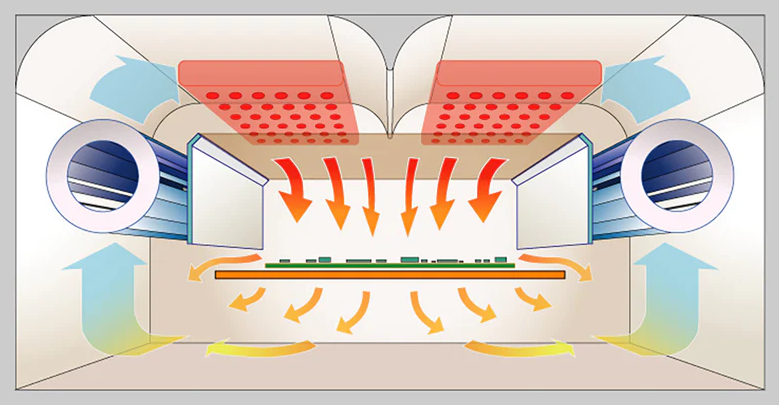
The history of reflow soldering dates back to the 1970s, evolving from basic wave soldering techniques to more sophisticated infrared-based systems in the 1980s. Initially developed to handle surface-mount technology (SMT) components, infrared reflow soldering gained prominence as semiconductor devices miniaturized. By the 1990s, it became integral to high-volume production, addressing the need for precision in attaching tiny chips and power modules. Today, in 2025, infrared reflow soldering continues to advance, incorporating smart controls and hybrid systems for even greater accuracy.
At its core, infrared reflow soldering involves applying solder paste—a mixture of flux and metal alloy particles—to PCB pads, placing components, and then exposing the assembly to infrared lamps or heaters. The infrared energy causes the paste to reflow, creating metallurgical bonds. This method is particularly suited for semiconductor packaging due to its ability to handle delicate materials like silicon wafers and gallium nitride (GaN) substrates without excessive thermal stress.
One key distinction in infrared reflow soldering is its radiant heat mechanism, which differs from convection reflow soldering that uses hot air circulation. Infrared waves directly excite molecules in the solder and board, leading to rapid heating. This selectivity minimizes overheating of sensitive components, a common issue in older soldering technologies. As semiconductor packaging demands tighter tolerances—such as in flip-chip or ball grid array (BGA) assemblies—infrared reflow soldering provides the control needed for sub-micron precision.
In practice, infrared reflow soldering ovens vary from benchtop models for prototyping to inline systems for mass production. These ovens often feature zones with adjustable infrared emitters, allowing operators to tailor heat profiles. For instance, modern infrared reflow soldering equipment can integrate vacuum environments to further enhance joint quality, as seen in specialized variants like the Vacuum Reflow Soldering Oven, which combines infrared heating with reduced pressure to minimize oxidation.
The adoption of infrared reflow soldering in semiconductor manufacturing stems from its compatibility with lead-free solders, mandated by environmental regulations like RoHS since 2006. Lead-free alloys, with higher melting points (around 217°C for Sn-Ag-Cu), require precise heating that infrared reflow soldering delivers efficiently. This evolution reflects broader industry shifts toward sustainable and high-reliability packaging.
Overall, understanding infrared reflow soldering begins with recognizing its role in bridging the gap between component placement and functional assembly. As we delve deeper, we'll explore how this technology specifically improves efficiency in semiconductor packaging.
How Does Infrared Reflow Soldering Work in Semiconductor Packaging?
Infrared reflow soldering operates through a structured process that ensures uniform melting and solidification of solder in semiconductor assemblies. The workflow starts with PCB preparation: solder paste is screen-printed onto pads using stencils, followed by automated pick-and-place machines positioning components like integrated circuits (ICs), resistors, and power transistors.
Once assembled, the board enters the infrared reflow soldering oven. Here, infrared lamps emit radiation in the 0.7–5 µm wavelength range, which is absorbed by the solder paste and PCB materials. This absorption converts radiant energy into heat, raising temperatures in a controlled manner. The process follows a standard temperature profile with four phases: preheat, soak (or thermal equilibrium), reflow, and cooling.
In the preheat phase, temperatures rise gradually from room level to 150–180°C at a rate of 1–3°C per second. This activates the flux in the solder paste, removing oxides and preparing surfaces for wetting. Infrared reflow soldering excels here due to its direct heating, avoiding the lag associated with convection methods.
The soak phase maintains 150–200°C for 60–120 seconds, allowing even temperature distribution across the board. In semiconductor packaging, this is critical for preventing warpage in thin substrates or thermal shock to delicate dies. Infrared reflow soldering's radiant nature ensures components with varying thermal masses heat uniformly.
The reflow phase peaks at 220–260°C for 20–40 seconds, melting the solder alloy. For lead-free pastes, peaks reach 245–250°C. Infrared energy focuses on the joints, minimizing overall board exposure. In applications like IGBT packaging, where large power devices require void-free bonds, infrared reflow soldering integrates well with fluxless or formic acid-assisted processes.
Cooling follows at 2–4°C per second to solidify joints without defects like cracking. Controlled cooling in infrared reflow soldering prevents intermetallic compound overgrowth, enhancing joint reliability.
In semiconductor-specific contexts, infrared reflow soldering is adapted for hermetic sealing and multi-layer stacking. For example, in wafer-level packaging, infrared heaters enable precise reflow of micro-bumps. Equipment like the Vacuum Reflow Soldering Oven enhances this by evacuating air, reducing voids to below 5%.
Post-reflow inspection uses X-ray or acoustic microscopy to verify joints. Infrared reflow soldering's process repeatability makes it ideal for high-yield semiconductor lines, where efficiencies stem from minimized rework.
This detailed mechanism underscores why infrared reflow soldering is preferred for complex semiconductor packages, offering scalability from prototypes to volume production.
What Are the Key Advantages of Infrared Reflow Soldering for Efficiency?
Infrared reflow soldering offers several advantages that directly enhance efficiency in semiconductor packaging. First, its rapid heating capability shortens cycle times. Unlike convection ovens, which rely on air circulation and can take longer to stabilize, infrared reflow soldering delivers energy instantly, reducing preheat durations by up to 30%. This translates to higher throughput in manufacturing lines, where seconds per board accumulate into significant productivity gains.
Second, energy efficiency is a hallmark. Infrared radiation targets the assembly directly, minimizing heat loss to the surrounding environment. Studies indicate that infrared reflow soldering consumes 15–20% less power than convection methods, as there's no need for blowers or extensive insulation. In 2025, with rising energy costs, this advantage supports sustainable operations in semiconductor fabs.
Third, improved joint quality boosts overall efficiency by reducing defects. Infrared reflow soldering's uniform heating minimizes thermal gradients, lowering the risk of tombstoning or bridging. For semiconductor devices, this means fewer failures in reliability testing, cutting rework costs by 10–25%. In power device packaging, like IGBT modules, infrared reflow soldering ensures consistent bonds, enhancing thermal dissipation and device lifespan.
Fourth, flexibility in handling diverse materials is key. Infrared reflow soldering accommodates various solder alloys, including low-temperature options for heat-sensitive semiconductors. Its adaptability to board sizes and component densities makes it versatile for mixed-technology assemblies, common in modern chips with embedded passives.
Additionally, infrared reflow soldering supports inline integration, streamlining workflows. Automated systems with real-time monitoring adjust profiles on-the-fly, optimizing for variables like humidity or paste viscosity. This automation reduces operator intervention, further elevating efficiency.
Environmental compliance adds another layer. Compatible with lead-free processes, infrared reflow soldering aligns with global standards, avoiding penalties and enabling market access. Chengliankaida Technology Co., LTD, for instance, has contributed to advancements in this area through specialized equipment development.
In summary, these advantages—speed, energy savings, quality, flexibility, and compliance—position infrared reflow soldering as a cornerstone for efficient semiconductor packaging.
How Does Infrared Reflow Soldering Reduce Voids and Improve Reliability?
Voids—gas pockets in solder joints—are a major concern in semiconductor packaging, as they impair thermal conductivity and mechanical strength, leading to failures in high-power applications. Infrared reflow soldering addresses this through precise control over outgassing and solidification.
During reflow, flux volatiles evaporate, potentially trapping bubbles if heating is uneven. Infrared reflow soldering's radiant heat promotes gradual solvent release, reducing void formation. Research shows void rates drop to under 5% with optimized infrared profiles, compared to 10–15% in some convection setups.
In vacuum-assisted variants, like the Vacuum Reflow Soldering Oven , pressure reduction evacuates gases before solidification, achieving near-void-free joints. This is vital for IGBT and power devices, where voids can cause hotspots and reduced lifespan.
Reliability improves via minimized intermetallic layers. Infrared reflow soldering's short peak times limit diffusion, preserving joint integrity under thermal cycling. For semiconductors, this means better performance in automotive or aerospace environments, with MTBF (mean time between failures) increasing by 20–30%.
Best practices include using low-void pastes and multi-stage profiles. Infrared reflow soldering also enables fluxless options, like formic acid activation, further eliminating void sources.
Overall, by tackling voids at the source, infrared reflow soldering enhances the long-term reliability of semiconductor packages.
What Are the Best Practices for Implementing Infrared Reflow Soldering?
Implementing infrared reflow soldering effectively requires adherence to best practices tailored to semiconductor needs. Start with profile optimization: use thermocouples to map temperatures, aiming for a ramp-up of 2°C/s, soak at 170°C for 90s, and peak at 245°C for 30s in lead-free processes.
-
Solder paste selection is crucial—choose types with fine particles (Type 4 or 5) for dense packaging. Ensure stencil apertures match pad sizes to avoid excess paste, which causes bridging.
-
Oven maintenance involves calibrating infrared emitters quarterly and cleaning reflectors to maintain efficiency. For semiconductors, incorporate nitrogen atmospheres to prevent oxidation.
-
Monitoring tools like thermal imagers detect hotspots, while software simulates profiles for new designs.
-
Training operators on defect recognition—e.g., cold joints from underheating—prevents issues.
-
Finally, integrate quality checks: AOI (automated optical inspection) post-reflow catches anomalies early.
-
These practices ensure infrared reflow soldering delivers consistent, efficient results in semiconductor production.
How Does Infrared Reflow Soldering Compare to Convection Reflow Soldering?
Infrared reflow soldering and convection reflow soldering differ primarily in heat transfer: radiant vs. forced air. Infrared reflow soldering heats faster, ideal for quick cycles, but risks shadowing in dense boards. Convection provides even distribution, suiting complex assemblies, though slower and more energy-intensive.
Efficiency-wise, infrared reflow soldering reduces energy use by 20%, but convection minimizes voids in high-mass components. For semiconductors, infrared excels in precision packaging, while convection handles volume better.
Hybrid systems combine both, offering the best of worlds. Choice depends on board complexity and production scale.
What Are the Challenges in Infrared Reflow Soldering and Their Solutions?
-
Challenges in infrared reflow soldering include uneven heating due to material absorption variances, leading to defects. Solutions involve multi-zone ovens and profile adjustments.
-
Overheating sensitive semiconductors is another issue; mitigated by selective wavelength emitters.
-
Maintenance of lamps and void management require vacuum integration.
-
In 2025, AI-driven controls address these dynamically.
What Are the Latest Advancements in Infrared Reflow Soldering as of 2025?
As of 2025, advancements include AI-optimized profiles for real-time adjustments and NIR LED systems for energy-efficient, low-cost reflow. Vacuum hybrids reduce voids further, while IoT integration enables predictive maintenance.
These innovations enhance semiconductor packaging precision and sustainability.
How Does Infrared Reflow Soldering Impact the Environment and Energy Efficiency?
Infrared reflow soldering promotes energy efficiency by direct heating, cutting consumption 15–20% vs. alternatives. It supports lead-free processes, reducing toxic waste. Lower emissions align with green manufacturing goals.
Conclusion
Infrared reflow soldering stands as a transformative technology in semiconductor packaging, driving efficiency through precision and innovation. By understanding its principles and applications, manufacturers can leverage it for superior results.
Why Are High Reliability Electronic Components Critical in Modern Electronics?
Which Selective Soldering Station is Best for Your PCB Line?
Related Article

Explore laser packaging process routes for LiDAR and optoelectronics. Discover how vacuum eutectic soldering secures sub-micron alignment stability.
Laser Diode Packaging Technologies: From TO-Can to Silicon Photonics

Compare inline vs. batch vacuum soldering systems. Learn how vacuum reflow ovens optimize void-free welding for high-power semiconductor packaging.
Vacuum Soldering Process & Equipment Comparison: How to Achieve Automotive-Grade Low-Void Manufacturing

